


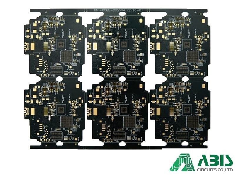
ABIS Circuits HDI PCB, 50–150 µm microvias, BGA pitch down to 0.25 mm, Any-Layer
ABIS Circuits HDI (High Density Interconnect) boards are produced with laser-drilled microvias and stacked or staggered vias. They suit fine-pitch BGA, mobile devices, 5G infrastructure and AI accelerators.
Available build-ups are 1+N+1, 2+N+2, 3+N+3 and Any-Layer HDI (ELIC), with resin-filled via-in-pad and sequential lamination. Materials include FR4, High-TG FR4, Rogers, Megtron and low-loss laminates; drilling by CO2 and UV laser.
Key features:
- Laser-drilled microvias
- Stacked/staggered microvias
- Resin-filled via-in-pad
- Sequential lamination
- Improved signal integrity
Specifications:
- Build-up types: 1+N+1, 2+N+2, 3+N+3, Any-Layer HDI (ELIC)
- Min. microvia diameter: 50–150 µm (laser drilling)
- Min. trace width: 50–75 µm (2–3 mils)
- BGA pitch: down to 0.25 mm
- Materials: FR4, High-TG FR4, Rogers, Megtron, Low-Loss
- Drilling method: CO2 + UV laser
- Microvia aspect ratio: 0.75:1 to 1:1
- Certification: ISO9001, ISO13485, IATF16949, UL, IPC-2226
Application: Smartphones, 5G infrastructure, AI processors, automotive ECUs, wearable electronics.
Before ordering: Before ordering, specify HDI build-up, BGA pitch, material, layer count and via filling requirements; provide Gerber files.
Specifications
| Brand | ABIS Circuits |
|---|---|
| Manufacturer part number | abis-002 |
| Country of origin | China |
| Product type | High-density interconnect (HDI) PCB |
| Model | HDI PCB |
| Application | Smartphones, 5G infrastructure, AI processors, automotive ECUs, wearable electronics. |
SKU: ABIS-ABIS-002